How Can You Validate Parylene Coverage?
Parylene XY is a transparent, thin (hundreds of nanometers to a few micrometers), well adhering, pin-hole and defect free conformal coating. They are coated uniformly on flat surfaces and component configurations with sharp edges, points, flat surfaces, crevices or exposed internal surfaces are coated uniformly without voids.
Why is Parylene tough to verify?
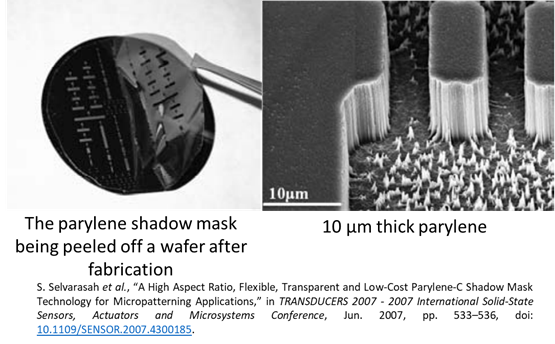
Because Parylene XY is transparent and forms a flawless / continuous layer its inspection becomes hard to the bare eye. Different types of inspection processes can be followed to verify the presence or uniformity of Parylene depending on which tools you have access to. The easiest at home inspection method is to inspect the de-masking lines. When a customer sends us a substrate for Parylene XY coating process, we receive a mask scheme along with other instructions. Masking process is necessary to protect the areas where Parylene XY must not be deposited. After the chemical vapor deposition process we carefully remove the masking material from the substrate without damaging the Parylene layer. Once the mask is removed edges of the Parylene conformal coating around the areas where a masked area and a coated area meet can be observed. You can perform this either with bare eye with a lot of care under light (watch for the reflection) or using an optical microscope (magnification) for ease. Spotting the de-masking lines is a very assuring way of validating the presence of parylene. In the Figure below, a Parylene layer being peeled off of a wafer and on the right hand-side 10 μm features are shown [1]. With a careful eye you can spot the Parylene layer from the edges on a macroscale.
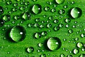
Parylene is a hydrophobic conformal coating meaning that if gets into contact with water the water will not spread but form semi-spheres on the Parylene surface. If your substrate or components will not be affected by water dropping a few drops of water on the areas where Parylene must be present would give a good idea of its presence. The dewetting angle of Parylene-AF4 is 100 degrees, Parylene C is ≈80 degrees and Parylene N is ≈75 degrees [2].
Other validation methods include electron microscopy and Fourier-transform infrared (FTIR) characterization by which you can obtain a high resolution image and a chemical fingerprint of the material, respectively.
REFERENCES
[1] S. Selvarasah et al., “A High Aspect Ratio, Flexible, Transparent and Low-Cost Parylene-C Shadow Mask Technology for Micropatterning Applications,” inTRANSDUCERS 2007 - 2007 International Solid-State Sensors, Actuators and Microsystems Conference, Jun. 2007, pp. 533–536, doi: 10.1109/SENSOR.2007.4300185.
[2] “(15) (PDF) Contact Angle of Parylene AF4 on a Sapphire Substrate,”ResearchGate. https://www.researchgate.net/publication/305905712_Contact_Angle_of_Parylene_AF4_on_a_Sapphire_Substrate (accessed Apr. 28, 2020).

随着电子产品防水需求的不断提高,从原先的 IP54到现在的IP67IP68等级!市场上出现了防水透气膜和防水透音膜,目前这两种不同的材料应用被搞混了,今天便与大家一起讨论防水透气
最近各地降雨量激增,所以手机就难免会沾点水,作为生活中不可或缺的电子产品,防水已经成为一个十分重要重要功能,而且个人对目前的IP68手机市场是相当不满意的。为什么?太贵
自然界中荷叶具有出淤泥而不染的典型不沾水特性(学术上称为Cassie-Baxter状态),具有自清洁、抗结冰、减阻、抗腐蚀等广泛应用价值,而玫瑰花瓣则具有水滴高粘附特性(称为Wenze
派瑞林各种粉材真空镀膜技术加工 纳米涂层防水处理
派瑞林各种粉材真空镀膜技术加工 纳米涂层防水处理
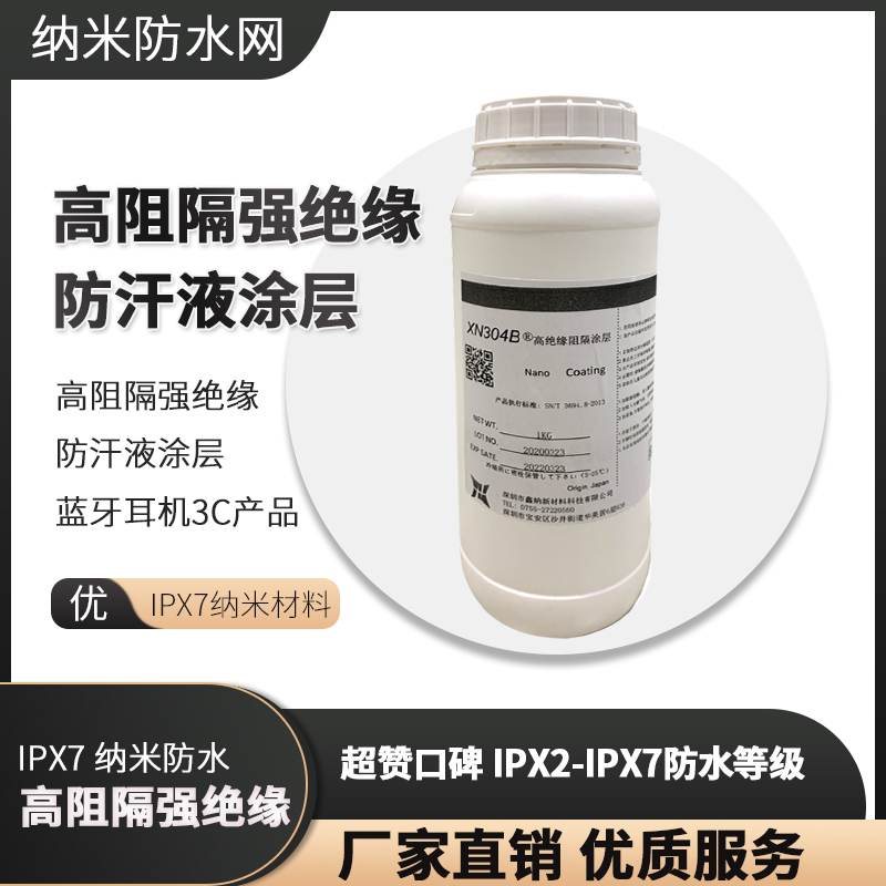
高阻隔强绝缘防汗液涂层蓝牙耳机3C电子产品IPX7纳米材料
高阻隔强绝缘防汗液涂层蓝牙耳机3C电子产品IPX7纳米材料
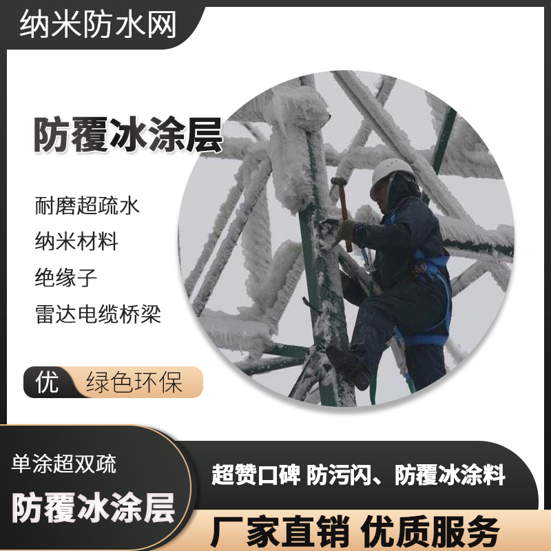
耐磨超疏水纳米材料 绝缘子架空导线电缆桥梁防覆冰涂层
耐磨超疏水纳米材料 绝缘子架空导线电缆桥梁防覆冰涂层
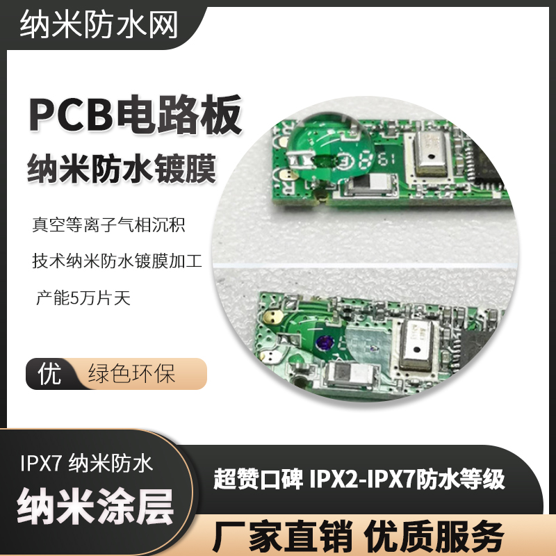
真空等离子气相沉积技术纳米防水镀膜加工 产能5万片天
真空等离子气相沉积技术纳米防水镀膜加工 产能5万片天
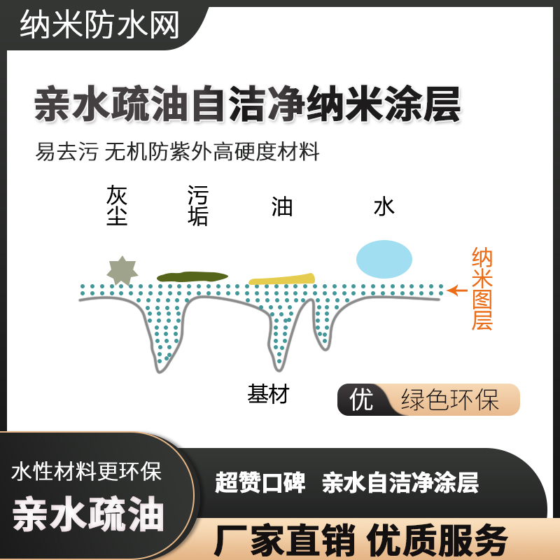
亲水疏油自洁净纳米涂层 易去污 无机防紫外高硬度材料
亲水疏油自洁净纳米涂层 易去污 无机防紫外高硬度材料
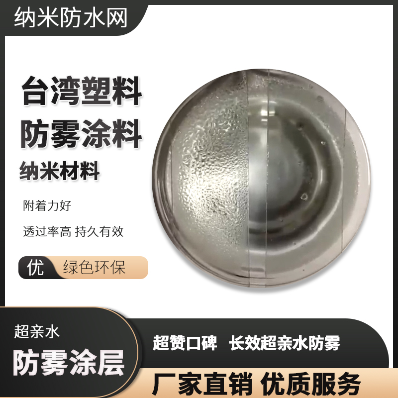
台湾超亲水防雾塑料专用 附着力好 透过率高 持久有效
台湾超亲水防雾塑料专用 附着力好 透过率高 持久有效


